Nand2Tetris 第 2 週 -- 布林算術
在第一週的作業中,我們從 nand 開始做出了Not, And, Or, Xor, Mux, DMux 等邏輯元件,並且進一步擴充為 Not16, And16, Or16, Mux16, Or8Way, Mux4Way16, Mux8Way16, DMux4Way, DMux8Way 的版本了。
但是,我們還沒讓電腦可以進行計算,特別是讓電腦作加減法,在這週的課程中,我們主要想做出一個完整的加法器,然後進一步做出 CPU 的心臟 -- 算術邏輯單元。
要做出 16 位元的加法器將兩個 16 位元的二進位數字 a[16],b[16] 相加起來,必須要能先做出 1 位元的二進位加法,這種將兩個位元相加的基礎元件稱為半加器,圖示與習題如下。

圖,半加器 HalfAdder
/**
 * Computes the sum of two bits.
 */

CHIP HalfAdder {
    IN a, b;    // 1-bit inputs
    OUT sum,    // Right bit of a + b
        carry;  // Left bit of a + b

    PARTS:
    // Put you code here:
}
但是,要能夠做出 16 位元的加法器,不能夠只拿兩個位元相加,而必須能夠進行三個位元的加法才行(因為可能會有進位)。因此我們需要能做三個位元相加的 FullAdder,以下是其電路圖與習題。

圖,全加器 FullAdder 的詳細電路
/**
 * Computes the sum of three bits.
 */

CHIP FullAdder {
    IN a, b, c;  // 1-bit inputs
    OUT sum,     // Right bit of a + b + c
        carry;   // Left bit of a + b + c

    PARTS:
    // Put you code here:
}
一旦我們設計出一個元件之後,就可以用方塊的方式表示它,只要將輸入輸出線拉出來就行了,以下是全加器的方塊圖。
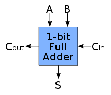
圖,全加器 FullAdder 的圖示
接著,我們可以串接很多個全加器,形成任意位數的加法器,以下是串接四個全加器所形成的四位元加法器。
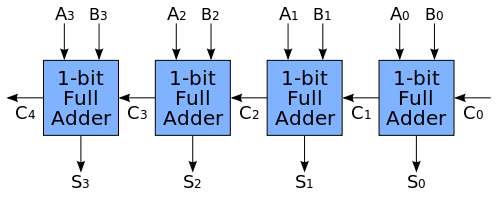
圖,用四個全加器建構出四位元加法器
當然,我們也可以做出更多位元的加法器,在以下習題裏就要求我們做出 16 位元的加法器。
/**
 * Adds two 16-bit values.
 * The most significant carry bit is ignored.
 */

CHIP Add16 {
    IN a[16], b[16];
    OUT out[16];

    PARTS:
   // Put you code here:
}
一旦你做出了 16 位元的加法器,那就可以輕易的做出 16 位元的遞增器 Inc16.hdl
/**
 * 16-bit incrementer:
 * out = in + 1 (arithmetic addition)
 */

CHIP Inc16 {
    IN in[16];
    OUT out[16];

    PARTS:
   // Put you code here:
}
然後就是本章的重頭戲,運用這兩章的元件做出一個完整的算術邏輯單元,其功能要求與作業內容如下。
/**
 * The ALU (Arithmetic Logic Unit).
 * Computes one of the following functions:
 * x+y, x-y, y-x, 0, 1, -1, x, y, -x, -y, !x, !y,
 * x+1, y+1, x-1, y-1, x&y, x|y on two 16-bit inputs,
 * according to 6 input bits denoted zx,nx,zy,ny,f,no.
 * In addition, the ALU computes two 1-bit outputs:
 * if the ALU output == 0, zr is set to 1; otherwise zr is set to 0;
 * if the ALU output < 0, ng is set to 1; otherwise ng is set to 0.
 */

// Implementation: the ALU logic manipulates the x and y inputs
// and operates on the resulting values, as follows:
// if (zx == 1) set x = 0        // 16-bit constant
// if (nx == 1) set x = !x       // bitwise not
// if (zy == 1) set y = 0        // 16-bit constant
// if (ny == 1) set y = !y       // bitwise not
// if (f == 1)  set out = x + y  // integer 2's complement addition
// if (f == 0)  set out = x & y  // bitwise and
// if (no == 1) set out = !out   // bitwise not
// if (out == 0) set zr = 1
// if (out < 0) set ng = 1

CHIP ALU {
    IN
        x[16], y[16],  // 16-bit inputs
        zx, // zero the x input?
        nx, // negate the x input?
        zy, // zero the y input?
        ny, // negate the y input?
        f,  // compute out = x + y (if 1) or x & y (if 0)
        no; // negate the out output?

    OUT
        out[16], // 16-bit output
        zr, // 1 if (out == 0), 0 otherwise
        ng; // 1 if (out < 0),  0 otherwise

    PARTS:
   // Put you code here:
}
這個 ALU 將會是 HackCPU 處理器的心臟,也可以說是這門課最重要的一個元件了。
注意事項
但是,在實作之前建議各位先閱讀一下 Nand2tetris 課程提供的 HDL Survival Guide 文件,這對您會很有幫助。
其中有幾點要注意的,筆者在此先提醒大家。
首先是 HackHDL 的輸入裏不能使用 0, 1, 但是可以使用 false, true ,其中的 true 代表一個全數為 1 的真值,傳入陣列輸入的話,就會變成 11111.... ,而 false 則代表 00000.....
注意下列範例,您可以將某些線路分別輸出或輸入
另外,我們可以用 a[4..11] 這樣的語法取出或設定 a 中第 4 到 11 位元的內容,如果是像 Or8Way (in=notIn[4..11], out=out) 這樣的語句,那就是將 notIn[4..11] 共 8 個位元取出傳入 in 線路當中,但是如果用 Something16(in=in, out[4..11]=notIn) 這樣的語句,則是將 notIn 傳入到 out[4..11] 線路當中,兩者的意義是很不相同的,以下是 HDL Survival Guide 裏節錄的一段說明,提供給讀者參考。
Sub-busing can only be used on buses that are named in the IN and OUT statements of an HDL file, or inputs and outputs of the chip-parts used in the PARTS section. If you need a sub-bus of an internal bus, you must create the narrower bus as an output from a chip-part. For example:

    CHIP Foo {
       IN in[16];
       OUT out;
    PARTS:
       Something16 (in=in, out=notIn);
       Or8Way (in=notIn[4..11], out=out);
    }

This implementation causes an error on the Or8Way statement. This needs to be coded as:

       Something16 (in=in, out[4..11]=notIn);
       Or8Way (in=notIn, out=out);

Multiple Outputs

Sometimes you need more than one sub-bus connected to the output of a chip-part. Simply add more than one out= connection to the chip-part definition.

    CHIP Foo {
       IN in[16];
       OUT out[8];
       PARTS:
           Not16 (in=in, out[0..7]=low8, out[8..15]=high8);
           Something8 (a=low8, b=high8, out=out);
    }

This also works if you want to use an output of a chip in further computations.

    CHIP Foo {
    IN a, b, c;
    OUT out1, out2;
    PARTS:
       Something (a=a, b=b, out=x, out=out1);
       Whatever (a=x, b=c, out=out2);
    }
結語
現在建議您可以上去看看影片並且實作第二週的習題了,以下是課程網址。
課程網址: https://class.coursera.org/nand2tetris1-001/wiki/week_2
以下是第二週習題的題目網址,請務必盡可能靠自己的能力完成,這樣才能深度理解這些設計的實作方法。
雖然兩位老師請同學不要將解答上傳到公開網路上,但還是有人上傳了,所以如果您真的做不出來或卡住了,還是可以參考一下答案,以下是 havivha 所提供的參考答案!
筆者經過半天的奮戰,終於把第二週的功課做完了!
由於對 Nand2tetris 課程的 HDL 的語法不瞭解,還著實吃了一些苦頭,除錯了很久!
雖然如此, Nand2tetris 已經做得很好了,這些時間花得還是很值得!
編輯: 陳鍾誠 email: ccckmit@gmail.com